Latest News

  • Industry Cooperation

  • Publish Date:2026-09-30
NYCU Brings Advanced Chip Design Into the Classroom With Private Cloud Supporting Over 500 Students
NYCU Joins Taiwan’s First High School–University–Research Alliance to Cultivate Future Scientists
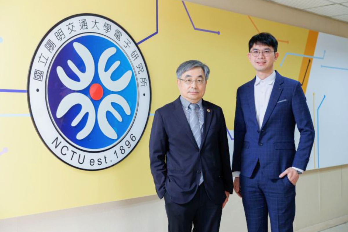
Ming-Dou Ker (left), associate dean of NYCU’s College of Electrical and Computer Engineering, and his doctoral student Lin-Hung Lai showcase an industry–university collaboration advancing cloud-based IC design education and semiconductor talent development. (Photo credit: AMD
 
______
National Yang Ming Chiao Tung University (NYCU) has built a private cloud platform that supports more than 500 students working simultaneously on chip design and simulation, bringing classroom training closer to the demands of the semiconductor industry. 

Developed with Bigstack and powered by servers equipped with AMD EPYC processors, the platform combines electronic design automation (EDA) tools with high-performance computing (HPC). It supports 18 integrated circuit (IC) courses, giving students mlhb hands-on experience in design workflows for advanced semiconductor processes.

The initiative receives support from Taiwan’s Ministry of Education under the Taiwan Chip-based Industrial Innovation Program. It addresses a growing challenge for semiconductor education: providing students with industry-relevant computing environments while protecting confidential design data and keeping systems manageable.

Meeting the Demands of Advanced Chip Design

As courses incorporate FinFET technology and advanced manufacturing processes such as 7-nanometer nodes, students need more than conventional circuit design training. They must also learn to work within increasingly complex design rules, software environments and security requirements.

Ming-Dou Ker, associate dean of NYCU’s College of Electrical and Computer Engineering, said the EDA tools and workflows used in teaching increasingly resemble those used in industry. That shift raises both computing demands and the need for tighter control over access to sensitive information.

Process models, design rules and process design kits (PDKs)—the files and data needed to design chips for a specific manufacturing process—contain confidential information. Supporting their use in teaching requires a private cloud with centralized management and isolated environments. Yet computing capacity was only part of the challenge.

“Our biggest problem was not hardware, but staffing,” said Lin-Hung Lai, who holds a doctorate from NYCU’s Institute of Electronics and planned the system. Graduate students previously had to maintain servers alongside their research responsibilities. A single host failure could disrupt classes for hundreds of students, making simpler administration a priority for the new platform.


Pooling Resources and Automating Routine Tasks

Built on Bigstack’s CubeCOS platform, the cloud consolidates previously separate computing resources into a shared pool. It provides isolated environments for different courses, balancing performance needs with access controls for confidential process data. The architecture also helps contain disruptions. When a node encounters a problem, maintenance can focus on the affected environment, reducing the risk of interruptions across the teaching platform.

To further ease the administrative workload, NYCU used Bigstack’s application programming interfaces (APIs) to develop its own Account Management System. The system automates account requests, activation, access permissions and password resets. Lai said connecting these processes through APIs has replaced substantial manual work with software, allowing the team to devote more time to teaching support and technical services.

NYCU currently operates 10 high-performance servers under unified CubeCOS management. The deployment supports concurrent design and simulation work by more than 500 students, with room to expand for more complex IC design courses and future AI applications.

Building Infrastructure for Long-Term Semiconductor Education

For Lai, a key outcome has been the close working relationship with a Taiwan-based technology team. “From hardware to software, we can discuss problems directly with engineers, and many issues can be resolved very quickly,” he said.

That collaboration has helped the university and its industry partner address practical teaching needs together, building expertise that extends beyond installing a new platform. Ker described the project’s central ambition: “We are not simply providing an experimental environment; we are building a laboratory.”

NYCU plans to continue expanding its computing capabilities for AI and advanced semiconductor design. The goal is to establish lasting infrastructure that supports teaching, research and closer connections with industry—and offers a model other universities can adapt as they modernize semiconductor education.
 
文章來源:DIGITIMES科技網

隨著FinFET、7奈米等先進製程逐漸成為半導體產業主流,人才培育也從傳統電路設計,進一步延伸至符合先進製程規範與雲端資安架構的大規模IC設計實作。如何讓學生在校期間就能接觸貼近業界真實流程的EDA(Electronic Design Automation)與先進製程設計環境,已成為大學的重要課題。

在教育部晶創計畫支持下,國立陽明交通大學搭載AMD EPYC處理器的高效能伺服器並攜手Bigstack以CubeCOS建構EDA/HPC(High Performance Computing)教學雲平台,打造可支援超過500名學生同時使用的私有雲環境,讓先進製程教學正式走入校園。

從先進製程教學到雲端管理 挑戰不只是算力

陽明交大電機學院副院長柯明道表示,隨著課程逐步導入FinFET等先進製程,學生需要使用的EDA工具與設計流程愈來愈接近產業現場,不僅運算需求大幅提升,環境管理與資安要求也更加嚴格。由於製程模型、設計規則與PDK(Process Design Kit)等資料涉及高度機密,校方必須建置具備隔離能力與集中管理機制的私有雲平台。

負責規劃系統的陽明交大電子所博士賴林鴻指出,相較於硬體設備,真正的挑戰其實來自管理人力。「我們最大的問題其實不是硬體,而是人力。」過去研究生除了研究工作外,還必須兼任系統維運,只要一台主機故障,就可能影響數百位學生上課,因此降低管理複雜度成為新平台建置的首要目標。

CubeCOS打造可規模化的先進製程IC設計教學雲

透過Bigstack建置的CubeCOS雲端平台,校方將原本分散的運算資源整合為統一資源池,並依課程需求建立兼顧效能與資安要求的多租戶隔離環境,讓機密製程模型(PDK)等資料能在不同課程環境間維持適當的存取隔離。當單一節點發生異常時,亦只需針對受影響的單一環境進行維護,不再影響整體教學服務,大幅提升系統可用性與維運效率。


除了資源管理外,Bigstack提供的開放API也讓陽明交大得以自行開發Account Management System(AMS),將帳號申請、開通、權限管理及密碼重設等流程全面自動化。賴林鴻表示,透過API串接,過去大量仰賴人工處理的行政流程已全面軟體化,讓有限的人力能更專注於教學支援與技術服務。

目前陽明交大已部署10台高效能伺服器,透過CubeCOS統一管理,支援18門積體電路相關課程及超過500名學生同步進行設計與模擬實作,也為未來更高複雜度的IC設計課程與AI應用預留擴充空間。

賴林鴻認為,這項計畫最大的收穫,不只是導入一套平台,而是與台灣團隊共同解決問題的合作模式。「從硬體到軟體,我們能直接和工程師討論問題,很多事情都能在很短時間內解決。」他認為,這樣的深度合作,累積的不只是技術成果,更形成教育與產業共同成長的生態系。

柯明道則以一句話總結整個計畫的核心精神:「我們不是在提供實驗環境,我們是在做實驗室建設。」

從建置教學雲平台到持續擴充AI與先進製程運算能力,陽明交大希望打造的不只是支援課程的系統,而是一套能長期支撐教學、研究與產業接軌的半導體人才培育基礎設施,也為台灣高等教育建立可複製的數位轉型典範。

Related Image(s):